Developing PCBs Using ExpressPCB
- Printed circuit boards (PCBs), which are specifically made for each circuit, come in handy. These are very compact and wire-free.
- . But for a normal hobbyist , purchasing a PCB from the shop for a specific circuit can be very expensive. So I searched for a way of making my own PCB in a simple way. I hope you will find this method interesting as it gives you the freedom to make your own customised PCBs
- All the required components are readily available at electronics hardware stores.
1. Draw the schematic of the circuit on a computer using the required software
2. Design the PCB on the computer using the required software
3. Print the PCB design through a laser printer
4. Take the impression of the circuit on a copper-clad board
5. Remove the excess copper by etching
Drawing the schematic
- There are many software available on the Internet to help you draw the schematic of the circuit.
- Eagle software is a very good option but it is not a free ware.
- So here we will use ExpressSCH for drawing the schematic. ExpressPCB(which includes ExpressSCH) is available on the Internet for free.
Circuit description-
- Let us assemble a simple buffer circuit using the 74HC244 buffer IC. We will put a tap switch at one input and see that we get the same output as the input by putting an LED light at the output pin.
- So when we push the switch to ‘on’ position the LED will glow, and when we push it to ‘off’ position the LED will turn off.
- Fig. 1 shows the screen shot of the buffer circuit drawn in ExpressSCH software.
Screenshot description-
Icons marked 1 through 24 allow you to perform various tasks as follows:
1. Rotate the component as well as the text by 90°. It can also be used to rotate only the text
2. Rotate only the component by 90°
3. It is the component and symbol manager. All the components can be found here
4. Options. You can change the colour and dimensions of the screen as well
as the grid spacing and other options
5. Previous zoom. It resumes the previous screen shape
6. Zoom to fit
7. Zoom out
8. Zoom in
9. Undo
10. Save
11. Open
12. General-purpose pointer, select and moving tool
13. Zoom into selected area
14. Place a component. It will not open the library window
15. Place a signal or symbol level like the symbols of power supply and ground
16. Place a wire. All the connections are made using this icon
17. Place a corner in the wire, i.e., break a continuous line into two
18. Disconnect a wire from a component and connect it to the other
19. Make a rectangle for a new customised component. You can make any component which is not present in the library
20. Add a line into a customised component
21. Add a circle or arc in a new component
22. Place a new pin in a component
23. Place text
24. Snap to grid. By keeping this option ‘on,’ the wires will move and make angles at specific gap. This makes it easy to draw straight lines and designs. By keeping this option ‘off,’ you will be able to make highprecision angles in the circuit
 Designing the PCB-
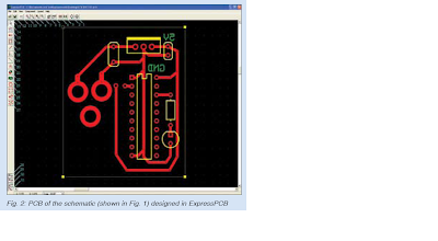
While designing a PCB, try to make it as compact as possible. Fig. 2 shows the PCB of the circuit (shown in Fig. 1) designed in ExpressPCB. Yellow lines show the silkscreen layer (component layout), red lines show the top copper layer and green portion is the bottom copper layer.
Rules of PCB making-
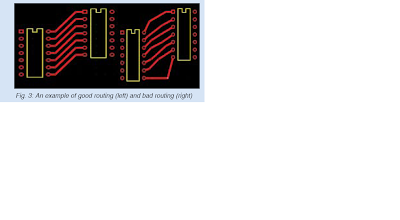
1. There should be no 90° connections of wires in the PCB. All connections should preferably be made at 45° (refer Fig. 3).
2. The mirror image of the PCB layout will always be imprinted on the copper side (the solder side of the copper-clad board) of the actual PCB. So for any text to be written on the copper side, the text should be mirrored during layout design so that the text appears normal on the copper side of the PCB.
3. Always print from a laser printer. Printout from inkjet or any other printer will not work as it may not be sharp enough.
4. You can print on both top and bottom parts of the board, but here we will print text only on the top copper layer.
5. There are standards for using traces of different thicknesses for different purposes: (a) 0.6mm (0.025-inch) trace for single tracks (b) 1.3mm (0.050-inch) trace for power and ground tracks (c) 0.2mm to 0.4mm (0.010- to 0.015- inch) traces for going between IC and component pads
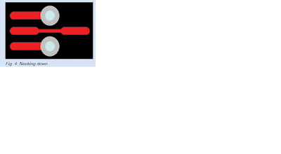
6. Tracking from large to small and then back to large is known as ‘necking’ or ‘necking down’ (see Fig. 4).
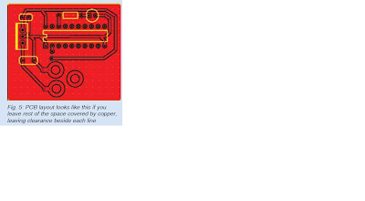
7. You can also let rest of the space remain covered by copper, leaving clearance beside each line, so our PCB will look as shown in Fig. 5. We will not use it as this type of filled circuit is best for industrial-level machine etching.
8. The standards for clearances for electrical conductors are listed here in the table (on previous page).
9. For thin tracks (<0.6mm> it is good to add ‘cham fer’ to ‘T’ junction, thus eliminating 90° angles
Printing the PCB layout-
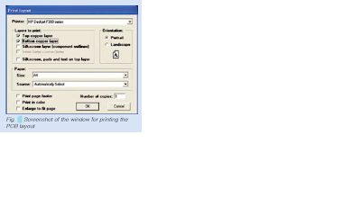
- Go to File→Print. A window as shown in Fig. 6 will open. Select ‘Layers to Print.’ Keep ‘Enlarge to Fit Page’ option unchecked as it will not give the exact layout of the components.
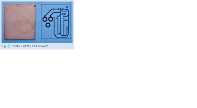
- Print the PCB layout from a laser printer. If you don’t have a laser printer at home, convert the file into a PDF file (using PDF995 software) and then print it elsewhere The printout of the PCB layout looks as shown in Fig. 7.
Etching-
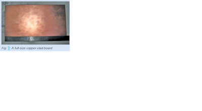
*Cut the copper-clad board to a size matching the size of the PCB design printout. You can also use a glass epoxy board but it’s costlier than a copper-clad board.Fig. 8 shows a full-size copperclad board.
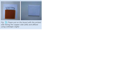
* Put the paper printout on the board with the printed side facing the copper side. Affix the paper to the board using cellotape so that the paper does not move while ironing (Fig. 9). Now take your household electric iron and set its temperature to the maximum (Fig. 10).
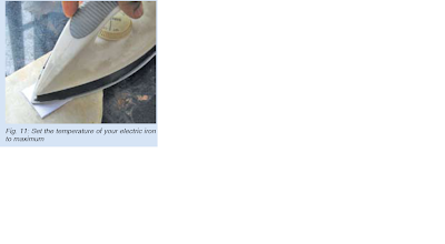
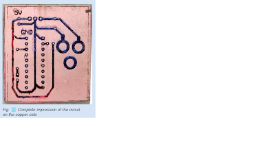
*Press the hot iron on the paper and carefully move it across the paper for about four minutes. While doing so, check for impressions. Continue ironing until the complete impression of the circuit comes on the copper side (Fig. 11).
* Complete the blanks, if any, with a good permanent marker. If any line is not dark enough, redraw it on the board using the permanent marker. Wash the board in normal tap water.
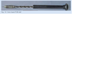
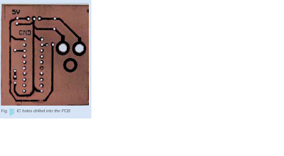
* Drill IC holes using a 1mm hand PCB drill as shown in Fig. 13. Redraw the lines using the permanent marker if they have been defaced by the drill.
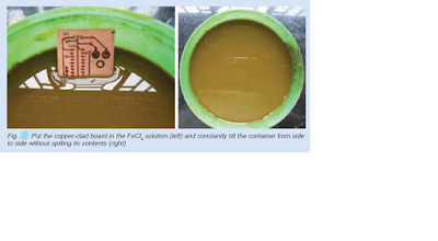
* Now mix some FeCl3 (ferric chloride) powder in hot water. The reaction is vigorous, so take safety precaution. Put the copper-clad board in the solution and constantly tilt the container from side to side without spilling its contents (Fig. 14). This is done to speed up the reaction. It takes five to six minutes to wash away all the excess copper.
*In between, keep checking the board. Ensure that the marker or carbon of the impression does not wash away.
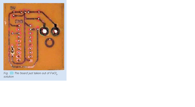
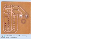
* Take the board out (Fig. 15) and wash it under tap water to remove the permanent marker ink. Remove carbon by using nail polish remover. Use a scrubber to gently scrub the copper surface (Fig. 16) till it shines.
* Your PCB is ready!


Hi fellas,
ReplyDeleteThank you so much for this wonderful article really!
If someone want to read more about that Express PCB I think this is the right place for you!
Hi fellas,
ReplyDeleteThank you so much for this wonderful article really!
If someone want to read more about that Express PCB I think this is the right place for you!